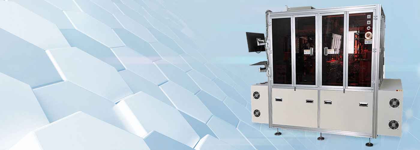
Mini LED VFC Die Bonder
A fully automatic high-speed needle punched VFC solidification device developed for Mini LED display technology and chip solidification process.
The grains on the crystal ring can be placed on the glued grain seat at high speed and precision, or pre placed on the glass carrier plate with laser welding film attached; Patent top pin visual common point design can reduce visual compensation time and improve crystal solidification rate.
Mini LED VFC Die Bonder
The grains on the crystal ring can be placed on the glued grain seat at high speed and precision, or pre placed on the glass carrier plate with laser welding film attached; Patent top pin visual common point design can reduce visual compensation time and improve crystal solidification rate.
Device parameters

CCD
CCD image positioning system, high-precision, high-speed linear motor and micrometer level marble platform, fully automatic loading and unloading system

Chip arrangement
Chip arrangement position accuracy(X/Y) <15μm

Max.Speed
0.045 sec/cycle
Avg.Speed
0.05sec/cycle
Device parameters
| Content | Specifications |
|---|---|
| Production efficiency | UPH 210K |
| Accuracy | (X/Y)< 20μm,σ<±3° |
| Die Size | 1mil×1mil~20mil×20mil |
| Wafer Frame | 204*204mm*1.0t |
| Substrate Size | 80×80mm-210×210mm(t0.1-2.5mm) |
| 9 | MITSUISEKI |
| 10 | OKAMOTO |
| 11 | Qinghong |
| 12 | Qinghong |
| Yield rate | >99.997% |